Block Diagram Of 2:1 Mux
Block diagram and circuit diagram of 3x1 mux Multiplexer in digital electronics Mux using multiplexers implement 8x1 logic multiplexer construct logical
Multiplexer in Digital Electronics - Javatpoint
Logic mux researchgate qca multiplexer Multiplexer electronics digital diagram truth table block javatpoint Multiplexer diagram circuit block inputs operation output selection lines types applications needed shown below data
8x1 mux logic diagram : using 8 1 multiplexers to implement logical
Mux 3x1 circuitMux selector gb bicmos consisting latches block Block diagram of the 2:1 mux ic.What is a multiplexer? operation, types and applications.
1 multiplexer design the pin diagram and functionDiagram multiplexer ic mux 8x1 table chegg function answered hasn expert ask question yet been 80-gb/s 2:1 mux consisting of five latches and a bicmos selector41 mux logic diagram : block diagram of 16 1 mux using four 4 1 mux.


1 Multiplexer design The pin diagram and function | Chegg.com
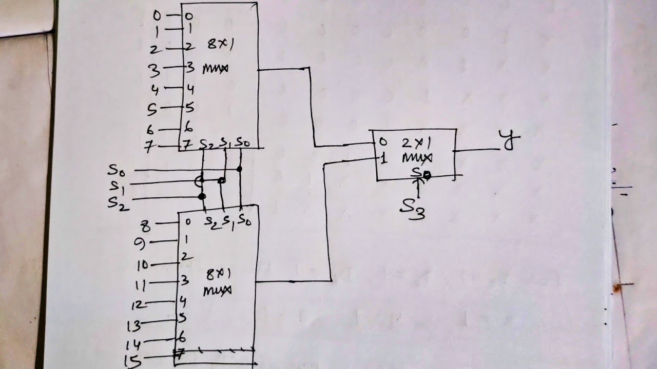
8X1 Mux Logic Diagram : Using 8 1 Multiplexers To Implement Logical

Multiplexer in Digital Electronics - Javatpoint

What is a multiplexer? Operation, types and applications

41 Mux Logic Diagram : Block Diagram Of 16 1 Mux Using Four 4 1 Mux

80-Gb/s 2:1 MUX consisting of five latches and a BiCMOS selector

Block diagram and circuit diagram of 3x1 MUX | Download Scientific Diagram